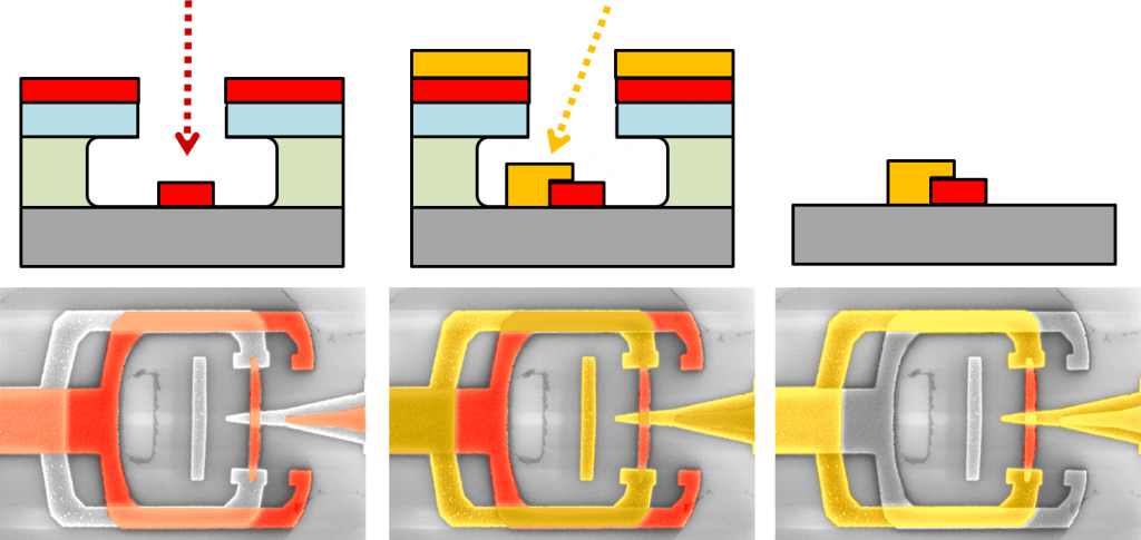
To realize devices which take advantages from the Josepson Junctions phenomenology, we need fabrication processes which allow to control the sample growth on tens nanometers scale. To reach such achievement we use the Shadov Mask Evaporation [1].
The Shadow Mask Evaporation (SME) is a common nano-fabrication technique by which high quality devices are obtained. The main steps of the process are:
- The device’s scheme is patterned on a silicon substrate coated with a bi-layer resist by the Electron Beam Lithography.
- Metal layer are deposited on the sample by multi-angle shadow evaporation. Insulator layer are growth by oxidation process, if needed.
- The bi-layer resist is removed.
The figure below shows an example of a multi-angle SME fabriction process. The upper part of the figure represents schematically the evaporation steps and the lift-off process. The lower part of the figure shows a series of Scanning Electron Micriscope (SEM) images about a proper SNS SQUID where aluminum and copper (yellow and red layer in the figure, respectively) are used as superconductor and normal metal, sepectively.

[1] G. J. Dolan. Offset masks for lift-off photoprocessing. Appl. Phys. Lett. 31, 337 (1977)