Partners
INFN Partners
INFN - Laboratori Naz. di Frascati
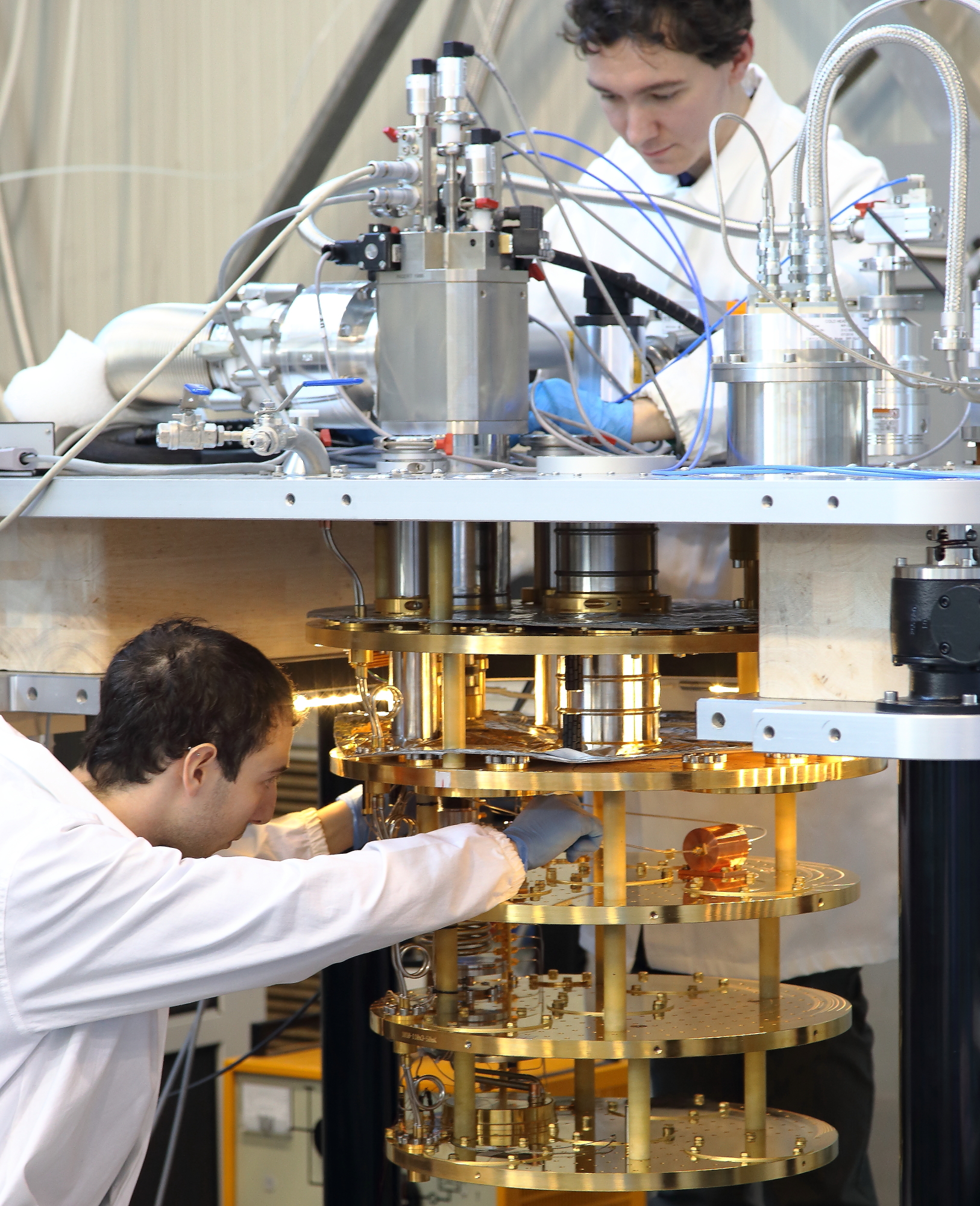
The INFN-LNF COLD (CryOgenic Laboratory for
Detectors) laboratory activities range from the characterization of cryogenic devices such
as normal and superconducting resonant cavities, to the R&D for
characterization of single photon detectors and Multi-harmonic magnetic
susceptibility measurement. Cryogenics main equipments includes a big-size
cryogen-free cryostat with a dilution refrigerator, a liquid Helium cryostat
with a compact plastic dilution refrigerator, and a liquid Helium cryostat
equipped with an 8 T SC magnet and a tuning system for cryogenic RF cavity
testing. The laboratory is also equipped with RF electronics and
instrumentation to perform measurement and characterization up to 20 GHz. The
COLD group is currently working on the QUAX, SQMS, DARTWARS, SAMARA and SUPERGALAX projects, and
proposed the FLASH experiment, all devoted to the Axion detection in the sub-eV
mass range.
INFN - Ferrara
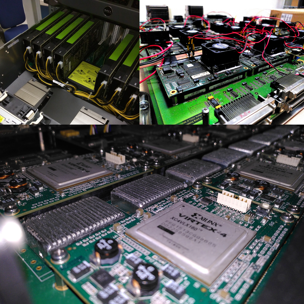
The INFN-Fe high performance computing group participates with the implementation of the software interface between the Qibo software framework and the SC qubit control and readout platform, built with FPGAs embedding RF ADCs and DACs.
The INFN Ferrara group has more than ten years of experience in highly parallel hardware architectures for the computation of complex lattice based simulations such as: Spin Glasses; Lattice-QCD and Lattice-Boltzmann simulations.
The group has been involved in the hardware design and implementation of highly parallel custom computing machines, as well as in the software implementation, porting and optimization of scientific applications, targeting custom and off-the-shelf compute devices, including FPGAs.
The group has been involved in several INFN projects such as SUMA, COKA and COSA, as well as EQC, and it is interested in the exploitation of quantum devices as accelerators in the context of scientific computing.
INFN - Firenze
INFN-Fi participates with a joint effort between the physics department and the department of information engineering. The activities in the physics department range from the development of quantum algorithms for simulating quantum many-particle systems, field theories and condensed matter systems, the control of transmon quantum devices, and the development of new sensing methods, exploiting also quantum machine learning techniques. The team has experience with the programming of near-term quantum devices via Qiskit, Amazon Braket, Pennylane and Yao.jl frameworks. The Department of Information Engineering (DINFO), is the University of Florence reference Department for ICT (Information and Communications Technology), where it carries out advanced research in control systems, computer science and engineering, electronics systems, electromagnetism, telecommunications, operation research, bioengineering and electrical engineering.
INFN - Milano-Bicocca
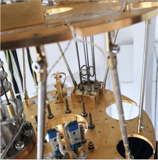
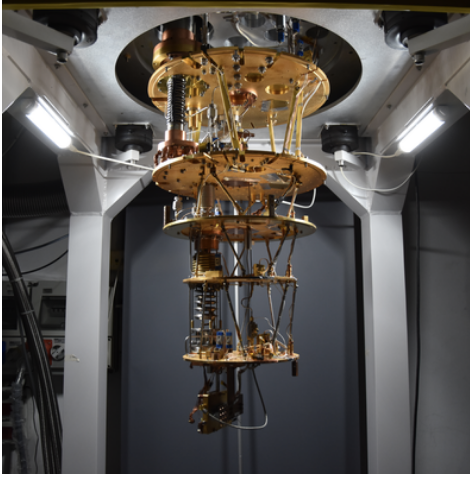
The INFN-MiB Cryogenic Laboratory is one of the largest and most advanced cryogenic facilities dedicated to research on low temperature detectors for particle and astroparticle experiments. All the facilities and infrastructures are jointly run with the University of Milano-Bicocca and with the Bicocca Quantum Technologies centre. The laboratory is fully equipped for low temperature detector testing as well as with vacuum and low temperature instrumentation, calibration sources, electronic instrumentation, microwave read-out, data acquisition systems, and instrument systems. The people directly involved in these activities have more than 20 years of experience in cryogenics, electronics, data acquisition, data analysis, and low temperature detectors thanks to the participation in national and international cryogenic projects for quantum technologies (DARTWARS) and for the study of the neutrino nature such as (HOLMES, MARE, CUORICINO, CUORE, CUPID, and KIDS_RD).
INFN - Milano
The INFN-Mi group is developing Qibo, a full stack open-source framework for quantum simulation, control and calibration, aiming to achieve hardware agnostic hybrid quantum operating system. Qibo is being developed for multiple institutions world wide from INFN (Italy) to IFAE (Spain), QRC (Abu Dhabi) and CQT (Singapore). The project started in 2020 with the development of language API for quantum circuits and a high performance classical simulator engine for quantum circuits based on hardware accelerators, such as GPUs obtaining one of the best performances for state vector simulation available at this time (2009.01845, 2203.08826). The Qibo framework is designed to accommodate multiple backends, i.e. optional modules which translate the quantum circuit representation into a practical implementation. We develop laboratory drivers to control the experiment through the modulation of microwave pulses, local oscillators, wave function generators and FPGAs. We provide modules for calibration, characterization and validation of qubits, including live plotting and automatic reporting tools.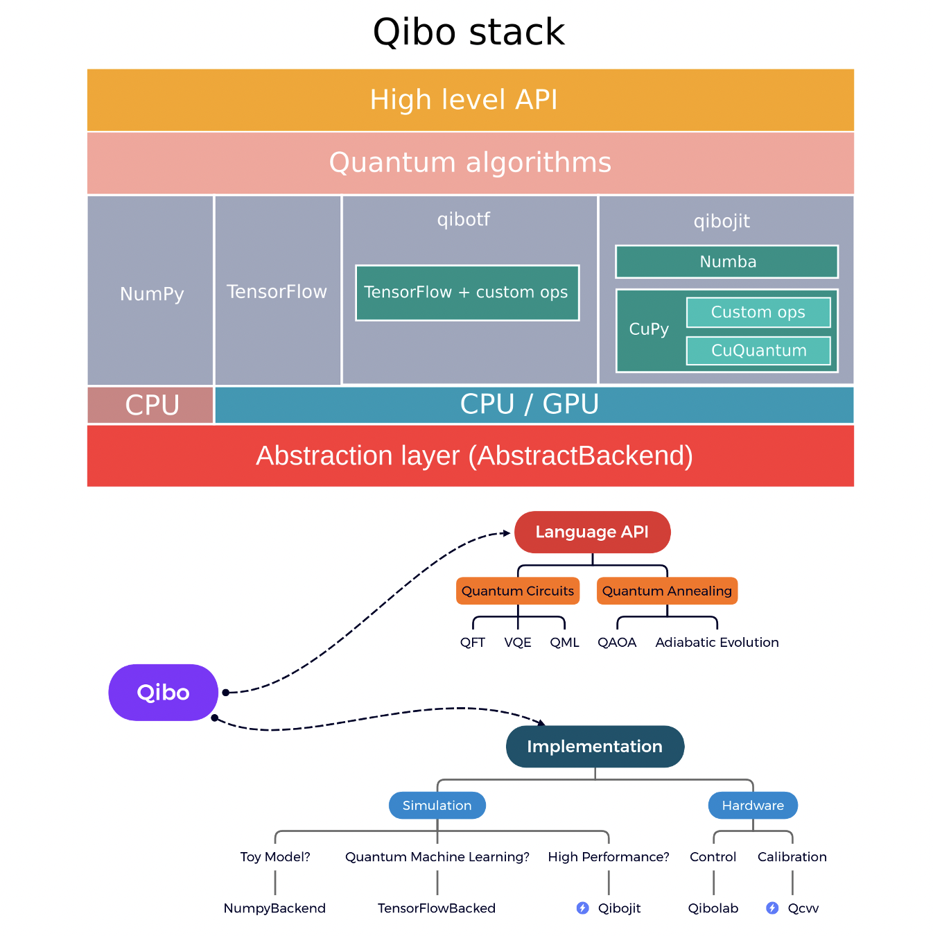

INFN - Pisa
The INFN-Pi unit contributes to all the activities of the Qub-IT R&D, including testing and measurements. The team is a collaboration between physicists and engineers of the Electronic and Computer Engineering Department. The physics group gained experience within SIMP in microwave-photon detection with TES and in simulation and realisation of antenna for signal collection in 3D structures., and the proposal of STAX, and experiment in the microwaves for the Axions and ALPS Search. The engineering group has know-how on measurements at mK temperatures, development of electronic systems and simulation and design of microwave circuits and will be involved in the development of the 3D Transmon. Pisa group is also collaborating with the NEST laboratories of the Scuola Normale Superiore the CNR superconducting and quantum electronics lab SQEL and the Physics Department of the University of Pisa optics and nanostructure group.
INFN - Salerno
The INFN-SA group has multi-decennial experience in simulation of JJ systems and in their experimental characterization in cryogenic lab. It has been involved in FEEL and SIMP experiments, and is currently operative in DARTWARS and VIRGO experiments. The team contributes, within QUBIT, to WP1-Design and WP4-Experiments. In particular it performs activities in modeling of the Josephson parametric amplifiers and optimization of the operational parameters (WP1-Tasks 1.2 and 1.3) and with experimental test of quantum circuit components to calibrate the fabrication process (WP4-Task4.1). Simulations exploit a fast workstation equipped with state of the art GPU for parallel computing. The experiments are performed using Oxford Instruments Heliox VL 3He system having 0.3 K base temperature and equipped with coax RF lines and a low noise cryogenic 1-14 GHz amplifier. Moreover, the laboratory is equipped with the following instrumentation: two 18 GHz microwave sources, a 20 GHz spectrum analyzer, a 9 GHz non sampling oscilloscope for transient analysis, a closed cycle cryogenic system with 3K base temperature, and a state of the art wedge and ball bonder.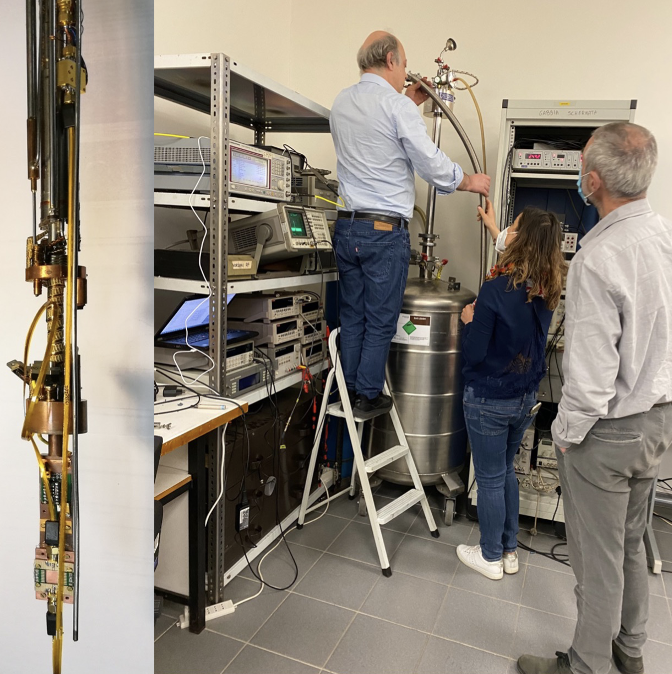

External Partners
CNR - IFN
The Institute for Photonics and Nanotechnologies of the National Research Council (IFN-CNR) carries out innovative research in the fields of photonics and of nanotechnologies pursuing both investigation of fundamental aspects and development of technological applications, with main focus on the research advancement in novel photonic and micro/nano-electronic devices and systems. IFN-CNR is tightly integrated with the national scientific community and collaborates with the major international Universities and Research Institutions through targeted projects funded by the major national and international agencies and foundations. The IFN-CNR Unit in Rome has a consolidated expertise in the development of electronic and optoelectronic devices, from design to fabrication and characterization, with specific focus on clean room processes and lithographic solutions. More specifically, present research focuses on the material deposition and micro/nano technologies for realizing advanced optoelectronic systems and solid state devices including integrated electronic components, sensors, optical coatings, bolometers and single-photon detectors, mems/nems, photonic crystals, and microfluidic devices. The institute has a long experience in the design, fabrication and characterization of superconducting devices such as Josephson junctions, SQUIDs, quantum boxes and single electron tunneling transistors, in particular for quantum applications and quantum computing. It has also a state of the art experience in the fabrication and optical characterization of integrated superconducting nanowire single photon and photon number resolving detectors
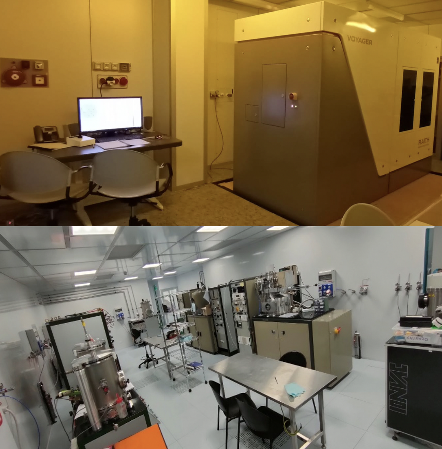
The research staff consists of 20 permanent employees. IFN-CNR has a Micro/Nanofabrication facility housed in a 300 sqm ISO6/ISO7 Clean-Room environment with state-of-the art equipments for thin films, materials and device processing, including electronic beam lithography (RAITH Voyager with acceleration voltage up to 50 kV), photolithography, thin metal film deposition (e-gun, thermal evaporation, sputtering, electroplating), dielectric and piezoelectric coating deposition (thermal evaporation and sputtering), wet and dry etching (multi-chemistry RIE, ICP-RIE for deep etching). Characterization and diagnostic tools including scanning electron (SEM) and atomic force (AFM) microscopes (morphology, current mapping and nanolithography), electrical probe stations for testing transport properties are also available in clean room environment.
FBK
The Sensors & Devices Center at Fondazione Bruno Kessler (FBK) focuses on the development and microfabrication of innovative devices, including superconducting quantum technologies for various applications, such as metrology and particle physics.
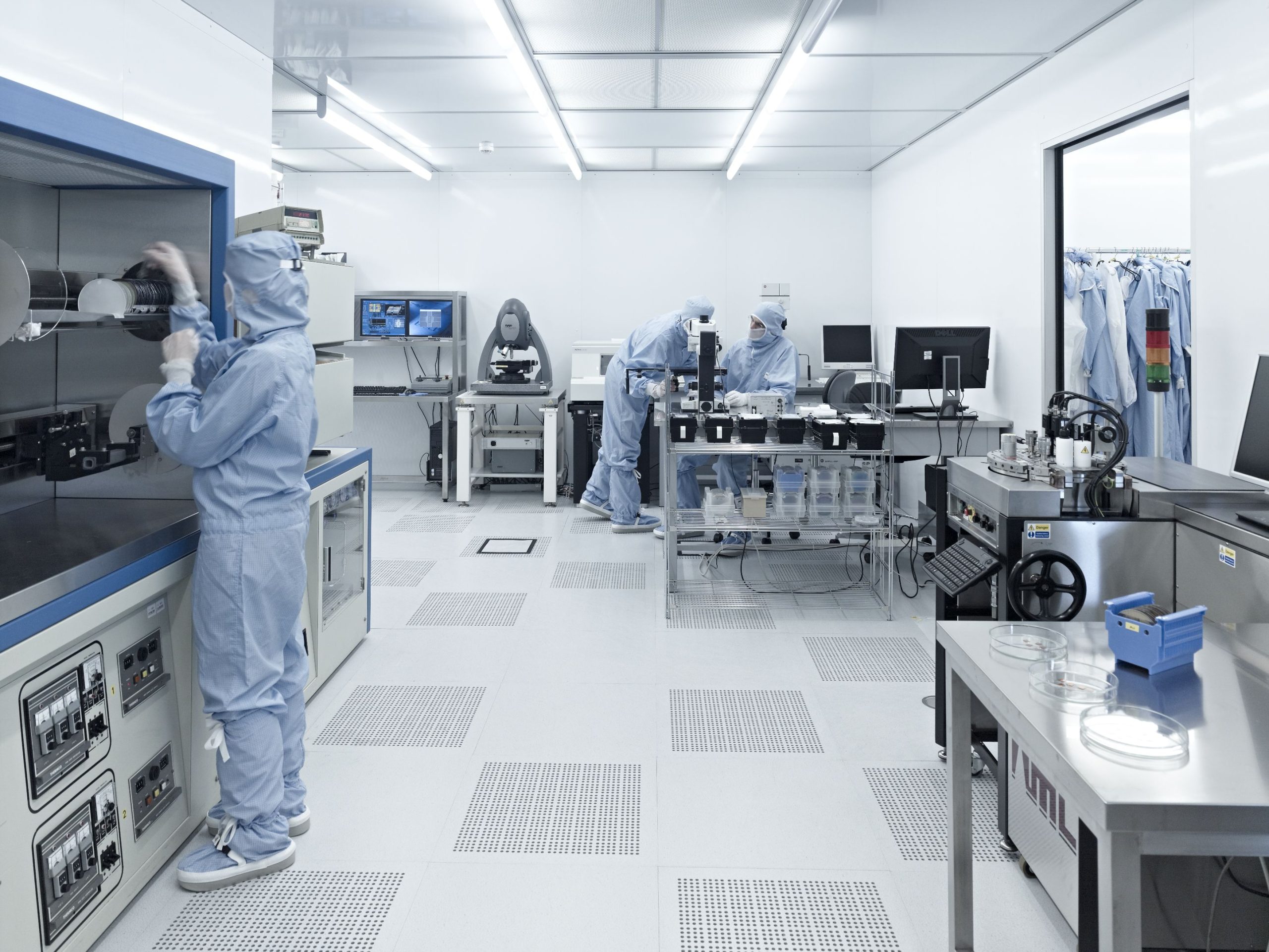
The microfabrication facilities available at FBK consist of three separate cleanrooms (classes 10/100, 100/1000, 1000) with a total area of about 1200 square meters.
The micro-nanofabrication processes include for example ion implantation, oxidation, Reactive Ion Etching (RIE), deep RIE, lithography (stepper 0.35 micron and mask aligner), sputtering, Focus Ion beam and Scanning Electron Microscope (FIB-SEM).
The cleanrooms also offer advanced technologies for structure characterisation, such as optical and mechanical profilometry, interferometry, etc.
Furthermore, a Testing Area of about 300 square meters with manual/automatic parametric testing, optical testing and test benches, as well as an Integration Area of about 100 square meters with microassembly station, bonding (ball/wedge bonder), pick and place, etc. are available.
Within the Qub-IT collaboration, the role of FBK is focused on the development and fabrication of Josephson junctions based devices, such as Josephson Parametric Amplifiers (JPAs).
[photo credits: Archivio fotografico Fondazione Bruno Kessler]