Advanced and innovative materials are the keys for future applications in sensors and quantum technologies, such as data storage and communication.
Materials with such characteristics can be obtained by implanting ions (charged particles) in a matrix, with the aim at achieving the so-called single photon emitters, or centers of color, which are able to absorb and emit radiations characterized by a specific wavelength.
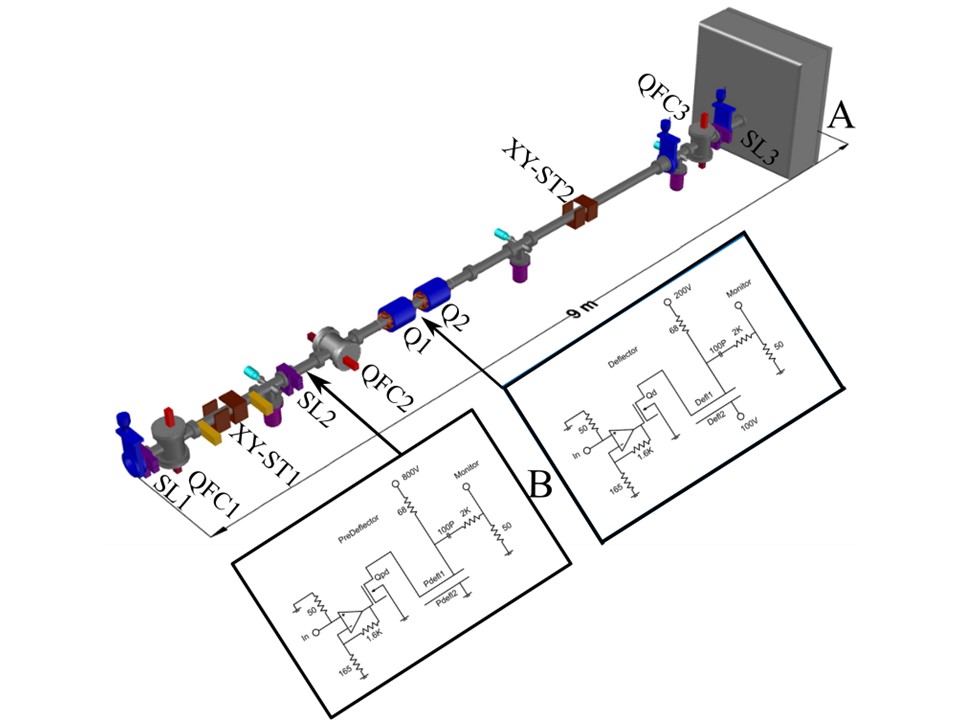
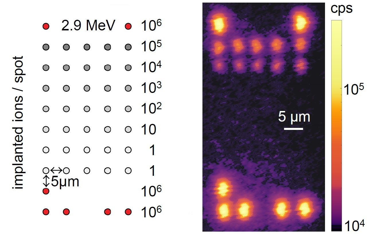
In the last few years, LABEC has focused on silicon (Si) ions implantations in diamond. The defects get in this way are the precursors for the formation of silicon-hole centers, which can be then activated by heating the material at high temperature (up to 1200°C) in high vacuum or in controlled atmosphere. The experimental setup makes it possible to realize implantations with different space resolution, so that different densities of created centers are possible, also using different fluences (i.e. total number of ions per irradiated surface unit), even up to get the transformation of diamond into amorphous material (the so-called graphitization of diamond).
Going into details:
– sample depth where implantation can be performed: 0 – 2.4 mm;
– possible incident ion fluences: 107-1015 ions per cm2;
– incident ions beam current: 10 nA/mm2;
– silicon-holes centers activation yield: 1-6%;
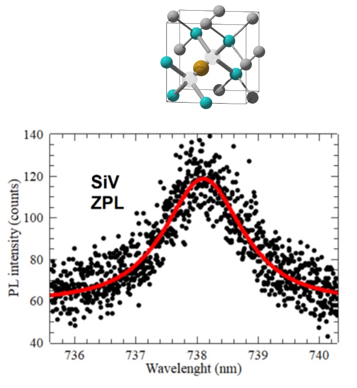
– single photon emitters characterized by short-time excited state (~1 ns), a strong zero-phonon emission line with a tight line width (~1.6 nm) at room temperature and a very small wavelength dispersion (0.015 nm), were achieved.