The Vertex Detector (VXD) of the Belle II experiment consists of two subdetectors: the Silicon Vertex Detector (SVD), a four-layer double-sided silicon-strip detector, and the Pixel Detector (PXD) consisting of two layers of pixelated DEPFET sensors. The PXD is the innermost detector. The VXD is reconstructs the production and decay vertices of the particles produced in the e+e- collision. It is crucial to perform time-dependent measurements, core of the Belle II physics program. The investigation of CP Violating processes requires to measure the decay time difference of the two B mesons produced in the collisions, the uncertainty on the measurement is dominated by the one on the measurement of the distance between the vertices (order of hundreds microns). The six-layer VXD allows to determine the position of the vertices with a precision better than 100 µm, allowing to reconstruct secondary vertices, i.e. the decay position of the particles coming from B decays, and also the tau and D mesons vertices, widening the Belle II physics program to charm and tau physics.
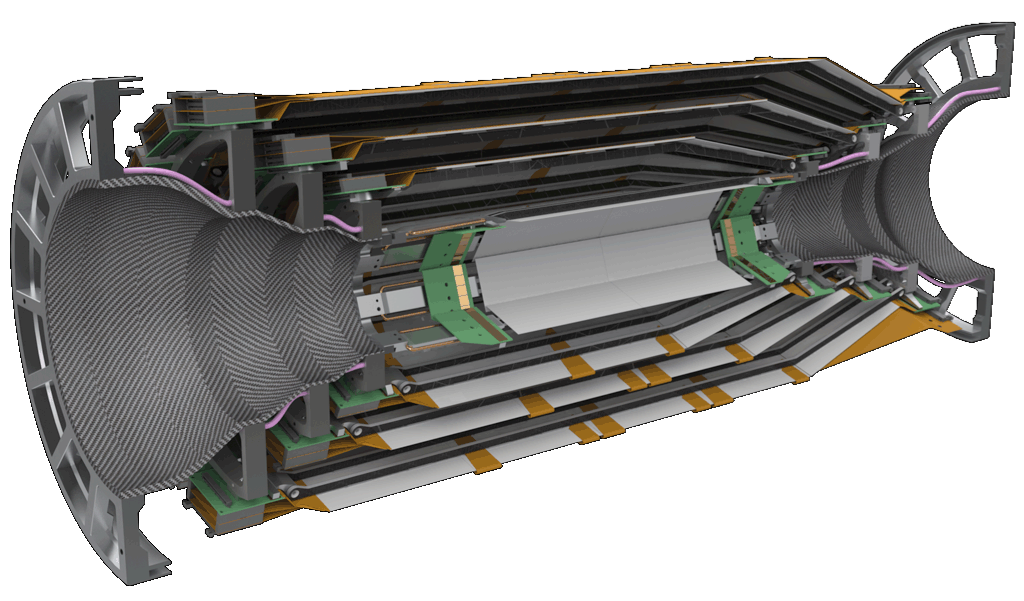
The SVD is shown in Fig 1, its design is based on the physics requirements (mainly the resolution on the impact parameter) and the background conditions expected at full luminosity. The charged-track transverse-momentum spectrum of a typical Belle II event ranges between tens of MeV/c and a few GeV/c, with an average of 11 of charged tracks. The main limiting factor for charged particle tracking is the multiple scattering. This fact puts a strong requirement on the material budget of the SVD (and PXD) layers. A second important factor for the design is the expected background-hit rate: with an increase of a factor 40 in luminosity, the hit rate will be sensibly higher than the previous B Factories. In order to keep the occupancy under control, shorter strips and a finer time granularity are necessary.

Fig 1: the Silicon Vertex Detector.
The SVD consists of 4 layers of Double-sided Silicon Strip Detectors (DSSD), with average radii ranging between 3.8 cm (layer 3) and 13.5 cm (layer 6), covering 90% of the solid angle. The SVD innermost layer consists of 7 flat ladders, each equipped with two silicon sensors for a total active area of around 470 cm2. The strips measuring the longitudinal direction (z) have a pitch of 160 µm, while for the measurement on the transverse plane the strip pitch is 50 µm. This pitch difference is due to the fact that the particles are boosted in the z direction. The three outer layers have a lampshade geometry with the slanted part in the forward region. This feature allows to reduce the material budget since the incident angle of the track is nearer 90 degrees for the boosted particles. Each slanted part of the ladder has one wedge sensor with a pitch of 240 µm for the longitudinal direction, and between 50 µm and 75 µm on the other side, for a sensitive area of 47 to 71 cm2. The flat parts of layer 4, 5 and 6 consist of 10, 12 and 16 ladders, each with 3, 4, 5 sensors per ladder respectively. The sensors pitches are 240 µm for the longitudinal measurement and 75 µm on the other side. There is an overlap (between 5% and 18%) among the ladders of a common layer, needed for the alignment procedures.
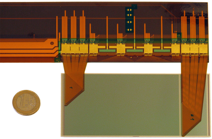
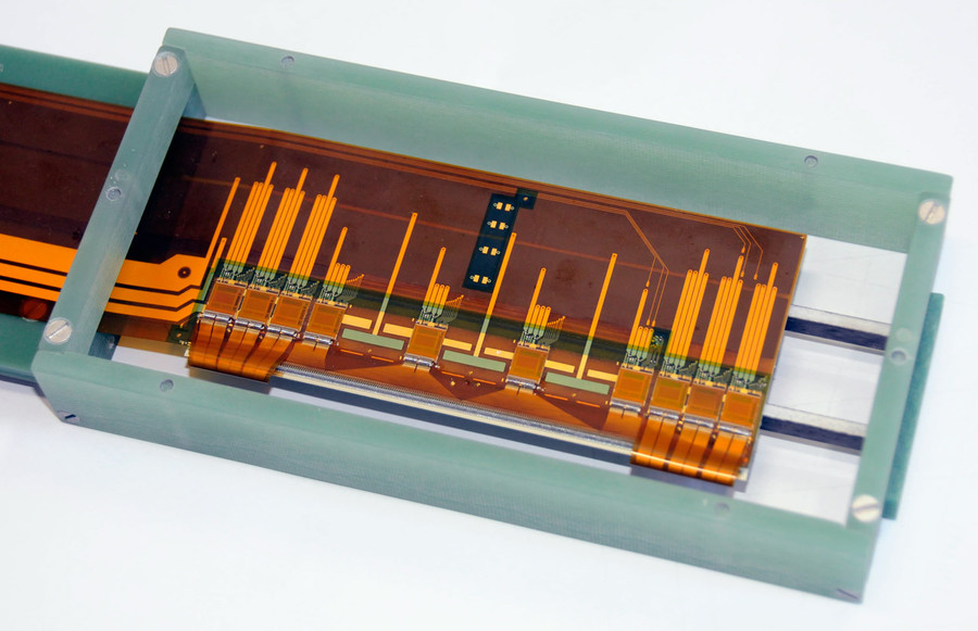
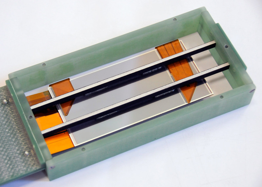
The readout of the sensors is performed by the APV25 readout chips, developed for the CMS experiment. Each chip can read 128 channels and has a short shaping time of 50 ns, important to keep a low occupancy. Due to the high background-hit rate expected on the SVD layers, each sensor is read independently by an APV25 chip. The readout electronics of the sensors at the boundaries of the tracking volume is placed outside the tracking volume itself, while for the rest of the sensors an origami-concept structure is adopted. The structure containing the APV25 is folded on the sensor, placing the readout electronics inside the active volume. In Fig 2 you can see a single module (sensor + readout) before folding. The two sides of the assembled origami module are shown in Figure 3.

Figure 2: A silicon sensor connected through two fan-outs to the APV25 readout chips, unfolded structure.


Figure 3: Assembled origami module in a transport frame (green). Top: readout side with APV25 chips, bottom: sensor side with structural ribs (black and white) and the flex circuits (orange) wrapped around the edge of the sensor.
The italian institutes involved in the SVD are the Istituto Nazionale di Fisica Nucleare (INFN) of Pisa and Trieste.


