Low Voltage System for GEM detectors
- Details
- Last Updated: Friday, 26 August 2016 12:29
|
Front End Electronics |
||
|
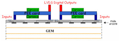
One of the major issue for a GEM detector is the electronics used for the signal readout. The electronics must have comparable performances on spatial resoulution (high density channels) and high rate capability. In the mainframe of LHCb (CERN) experiment, a Carioca GEM Chip has been designed and made for the signal readout of muon station chambers M1R1, just around the LHC beam pipe. Each chip has 8 channels with a sensitivity of 2-3 fC; The output are timeoverthreshold LVDS signals with a typical width of 10-30 ns. The chip is radiation tollerant; . |
||
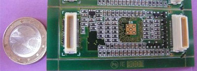 |
In Frascati we designed and made a Front End Board with two of these non-encapsulated Carioca Chips. The final "Carioca Card" is extremely modular and usable for different GEM applications with a total dimension of 3x6 cm2, with a channel density of 1 ch/cm2. |
|
 |
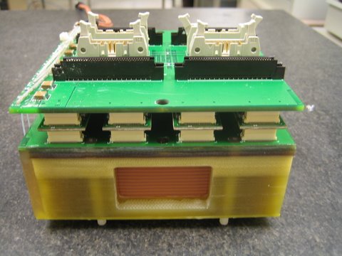
In this picture the cross section of a GEM detector with two Carioca Boards are visible. | |
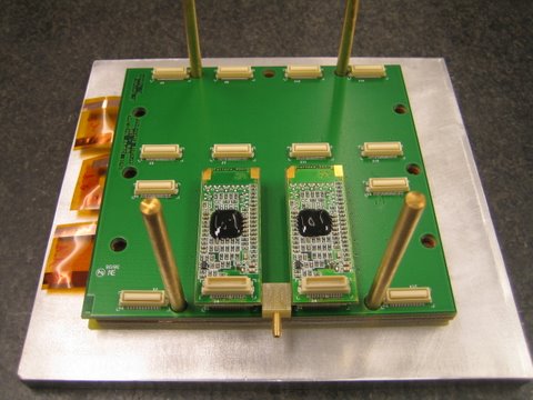 |
On the left, two Carioca Cards have been plugged on a GEM Chamber backplane. In general we use 8 Carioca Cards for each GEM detector for a total of 128 LVDS channels. |
|
|
|
A mother board can be easly plugged on top of the 8 Front End Boards |
|
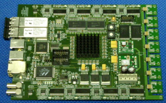 |
The second mother board is built with an FPGA on board able to acquire the 128 LVDS signals and measure : The "inteligent" mother board (see the picture aside) foreseen for data transfer both Here the link to the GEMBOARD Manual |
|