
Oltre il laboratorio: le sinergie tra INFN e realtà industriali nel campo dell’ Additive Manufacturing
Nel suo intervento a RM Forum, Pietro Rebesan, tecnologo della Sezione di Padova, parla delle...
9 Ottobre 2025
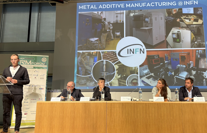
Nel suo intervento a RM Forum, Pietro Rebesan, tecnologo della Sezione di Padova, parla delle...
A SRF2025, INFN presenta il suo portfolio di nuove tecnologie per la realizzazione e la finitura del...
Il Comitato Nazionale per il Trasferimento Tecnologico dell’INFN cambia volto: Marco Statera pr...
Con il rinnovo per altri 3 anni dell’Accordo Quadro, si rafforza la collaborazione tra i du...

Il valore strategico dell’accesso esclusivo nella valorizzazione della ricerca pubblica L’esclus...

Il Comitato Nazionale per il Trasferimento Tecnologico (CNTT) dell’INFN si rinnova, accogliendo Gi...
Articoli, software, grafici, immagini: la produzione scientifica è fatta anche di opere creative. E...

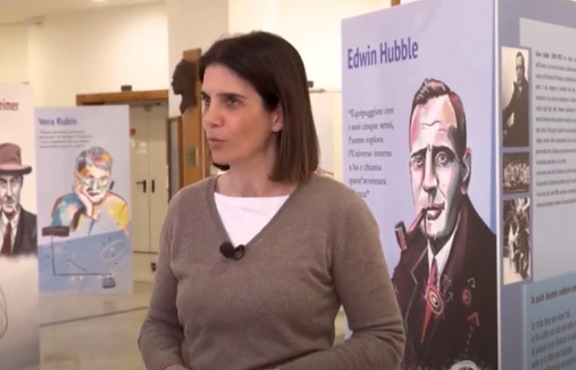
Una carriera costruita tra laboratori, collaborazioni internazionali e tecnologie per la salute: la ...
Dagli esordi come perito elettronico a imprenditore visionario passando per l’INFN: Marcell...
Quando la ricerca si traduce in valore, anche le parole contano Il trasferimento tecnologico ...
Dai Laboratori Nazionali di Frascati, ricerca scientifica e trasferimento tecnologico al servizio de...
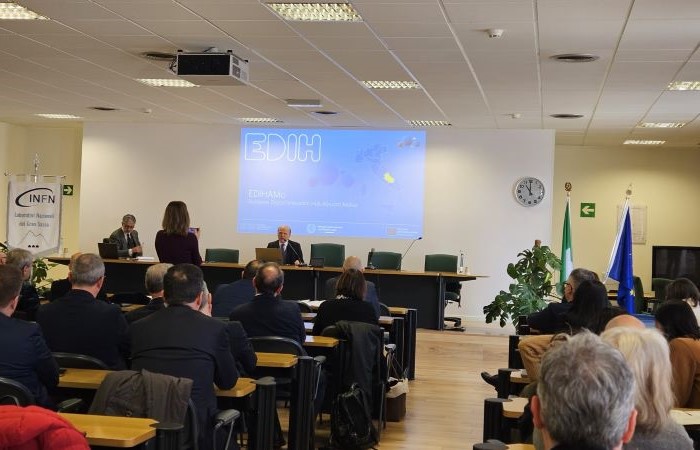
All’iSAS Padova Meeting, INFN porta la sua esperienza su efficienza energetica e trasferimento...
L’ex responsabile del Servizio di Trasferimento Tecnologico all’INFN racconta come si costruisce...
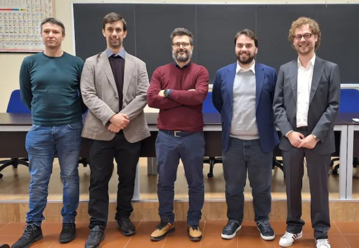
Laboratori Nazionali di Legnaro, 14/03/2025...

L’INFN ha stanziato 150.000 euro per finanziare progetti innovativi nell’ambito del trasferiment...
L’innovazione trova il suo pieno significato quando un’idea si trasforma in una soluzione concre...
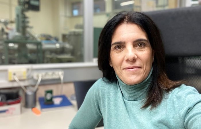
L’esperienza e il percorso di Mariangela Cestelli Guidi, Coordinatrice del Comitato Nazionale di t...
Occorre gestire la frammentazione fra i soggetti incaricati di favorire processi di innovazione tram...
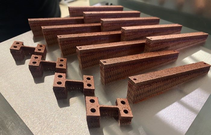
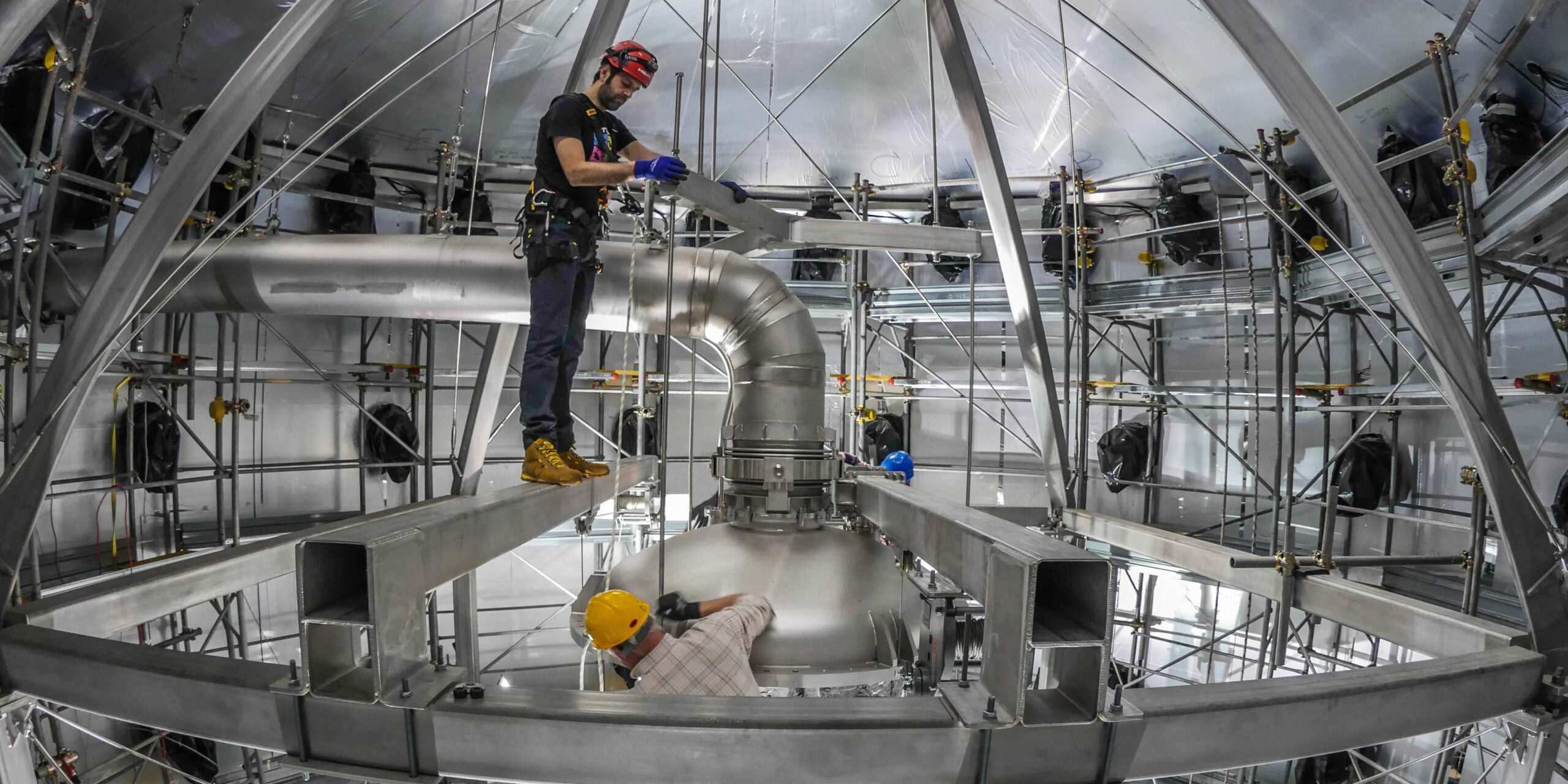
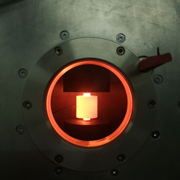
La manifattura additiva sta trasformando il panorama tecnologico, permettendo la creazione di materi...
La ricerca scientifica, oltre ad arricchire il patrimonio culturale dell’umanità, genera rica...
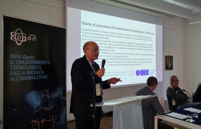
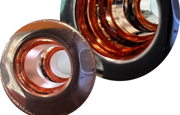
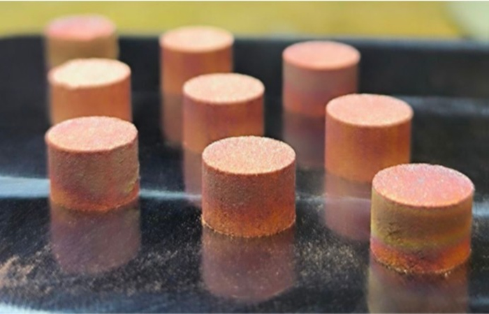
Valvole di nuova generazione per idrogeno liquido in grado di operare a temperature fino a -253°C. ...
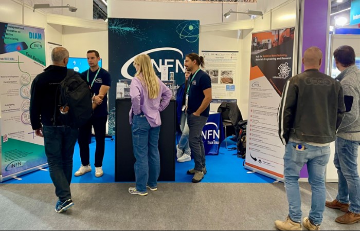
Innovazione e competenze al servizio della manifattura additiva Una presenza strategica per raccogli...
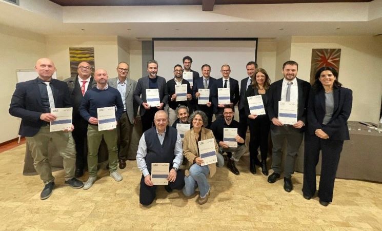
All’evento “Celebration” tenutosi a Frascati presentati gli otto progetti elaborati per raffor...
Francoforte, 19/11/2024 – 22/11/2024...
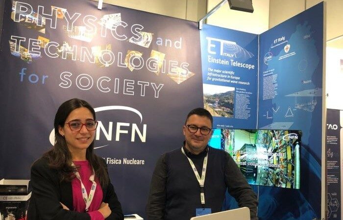
Dal 1° al 4 ottobre, presso il Generali Convention Center di Trieste, si è tenuta la terza edizio...
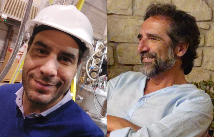
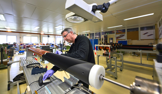
Antonio Carabillò, Production e R&D Manager di Eurolls S.p.A. ha recentemente conseguito i...
Palazzo Merulana, Roma, 18/09/204...
Come promuovere quello scambio proficuo tra ricerca e industria che porta nel nostro quotidia...
Sviluppare cure oncologiche avanzate con adroterapia di precisione ancora più veloci ed effi...
Isola d’Elba, 26/05/2024 – 01/06/2024...
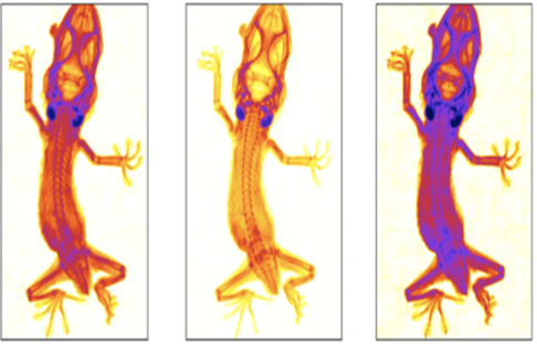
Per la prima volta un singolo cristallo di perovskite è stato utilizzato per rivelare e tracciare p...
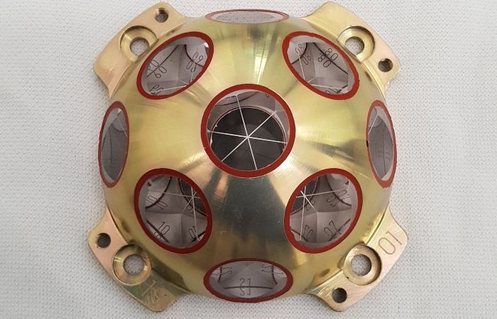
Realizzata da INFN per Eurolls Spa...
Movable Accelerator for Cultural Heritage In-situ Non-destructive Analysis, un acceleratore di parti...
Le tecnologie pionieristiche del progetto Hitriplus, sviluppate anche con la partecipazione di INFN,...
Scoprire e sviluppare nuove terapie antitumorali mediante piccole molecole note come Folding Interf...
Creare un ponte tra la fisica di base e il mondo produttivo: questa è la missione del Comitato Tras...
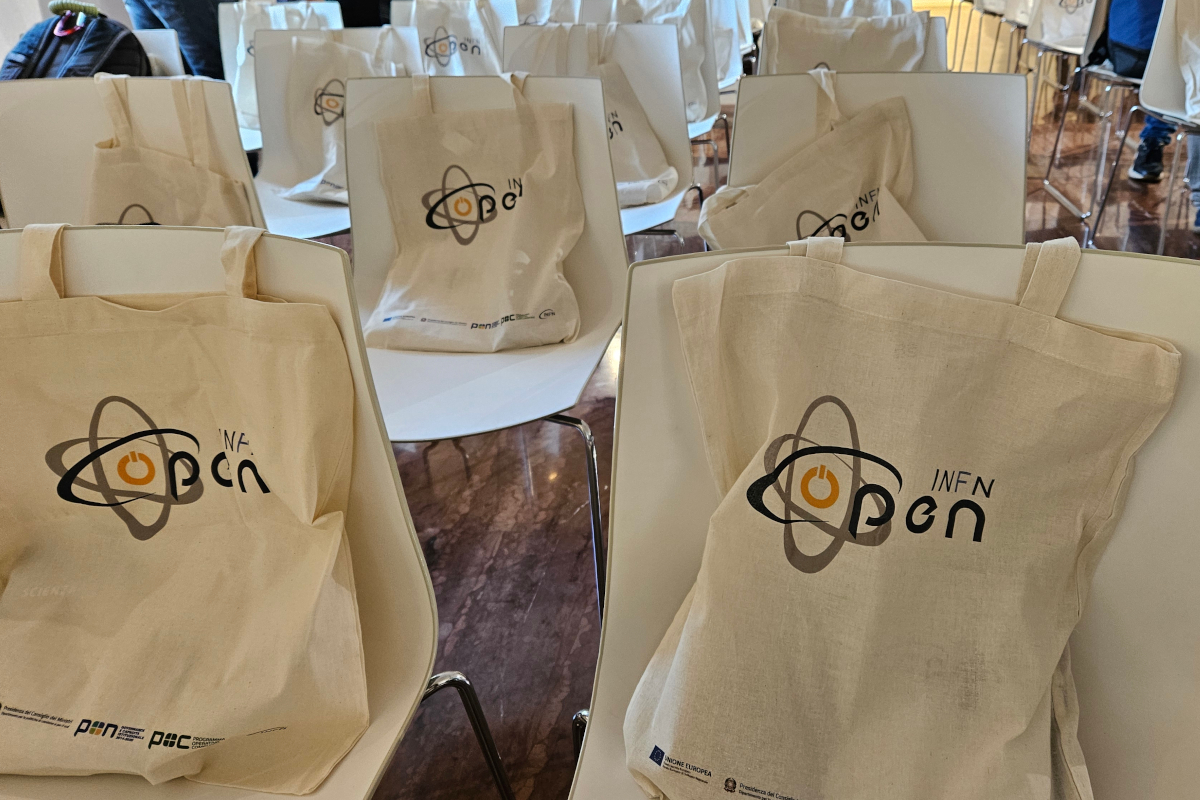
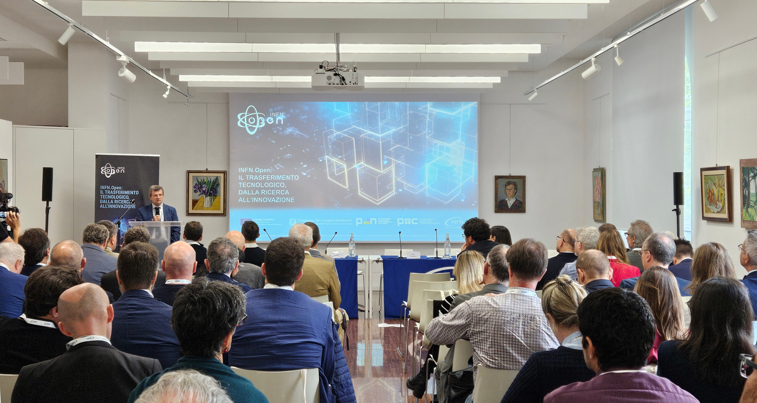
Tra i diversi sviluppi che sta ottenendo il progetto INFN.Open a un anno dall’avvio della sua fase...
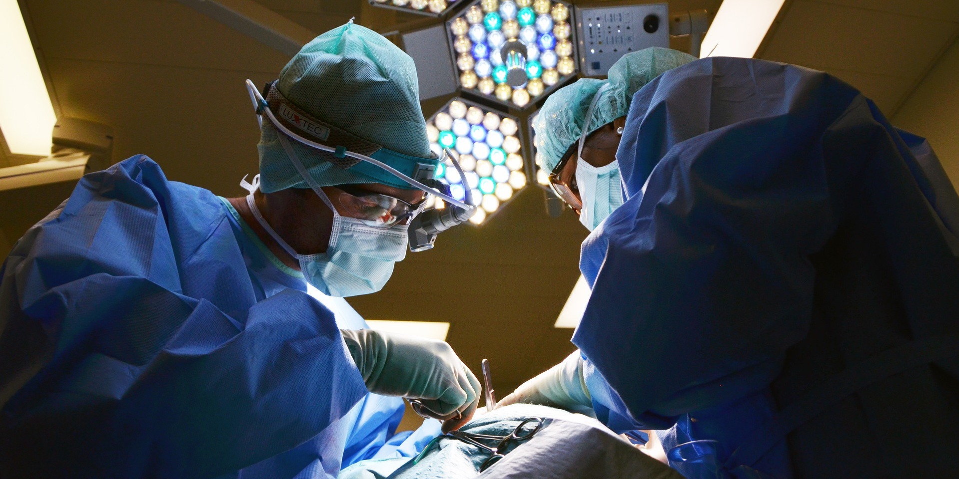
Sono iniziate le sperimentazioni in vivo di una sonda intraoperatoria per la chirurgia di precisione...
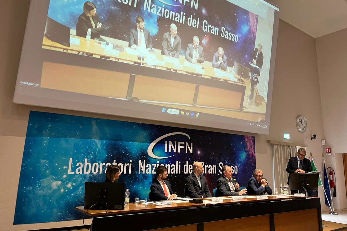
Laboratori Nazionali del Gran Sasso, 23/05/2023...
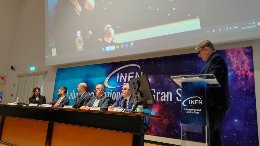
L’Aquila, 23 maggio 2023 – Si è svolto oggi, presso i Laboratori Nazionali del Gran S...

Il trasferimento Tecnologico di INFN sarà presente all’evento Innovation&Match che si svo...
Finanzierà progetti di sviluppo di tecnologie volti all’aumento del Technology Readiness Level e ...
Mettere a servizio della società le conoscenze scientifiche e tecnologiche generate dall’Istituto...
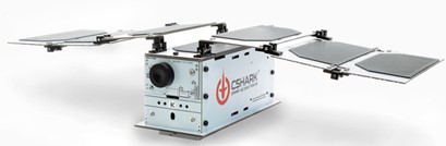
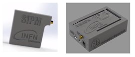
CShark ha in programma di integrare il rivelatore di radiazioni ArduSiPM, sviluppato dalla Sezione I...
Sono tre i progetti che godranno di un finanziamento volto a superare l’ “ultimo miglio&...
il Comitato Nazionale per il Trasferimento Tecnologico dell’INFN ha visitato il sito di Capo Passe...
Avviata una collaborazione tra la Sezione di Catania di INFN e ACOSET SpA per lo sviluppo di metodi ...
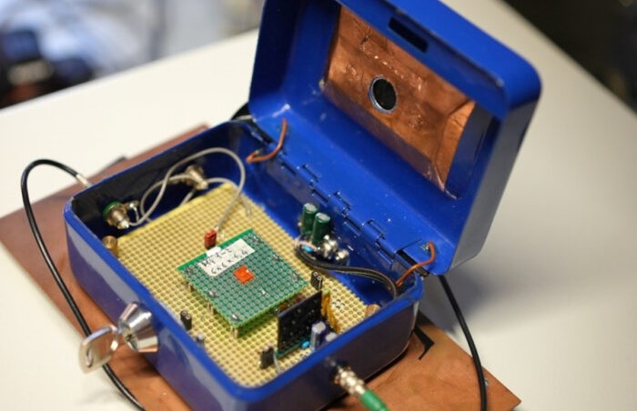
Le applicazioni sono molteplici: dai laboratori didattici, all’utilizzo come monitor di radiazioni...

INFN Perugia e CNAF sono fra i promotori del progetto Umbria Digital Data (UDD), per il bando riguar...
Finanzierà progetti di sviluppo di tecnologie volti all’aumento del Technology Readiness Level e ...
Finanziato con 1,7 milioni di euro, sarà interamente dedicato alla valorizzazione delle conoscenze ...
L’INFN ha siglato due accordi per la fornitura di 12 sistemi di riflessione laser che verranno...
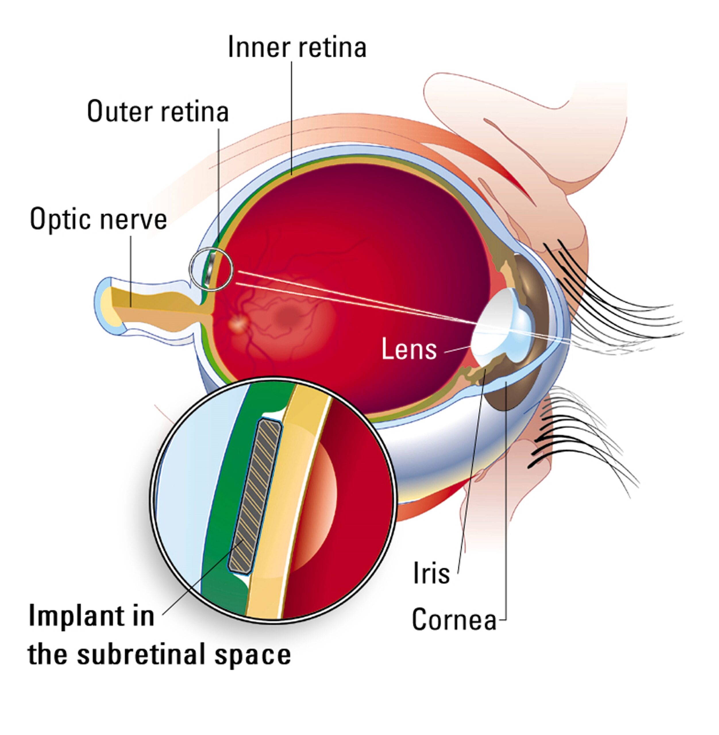
Il progetto SPeye di INFN vuole realizzare una protesi retinica impiantabile che permetta di salvagu...
Beamide S.r.l. è la nuova società spin-off dell’INFN che svilupperà software per simulare gli e...
TT_SINTER è un’apparecchiatura per la sinterizzazione che permette di trattare materiali trad...
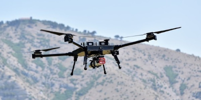
Battesimo dell’aria per il drone capace di identificare in real time le sorgenti radioatt...
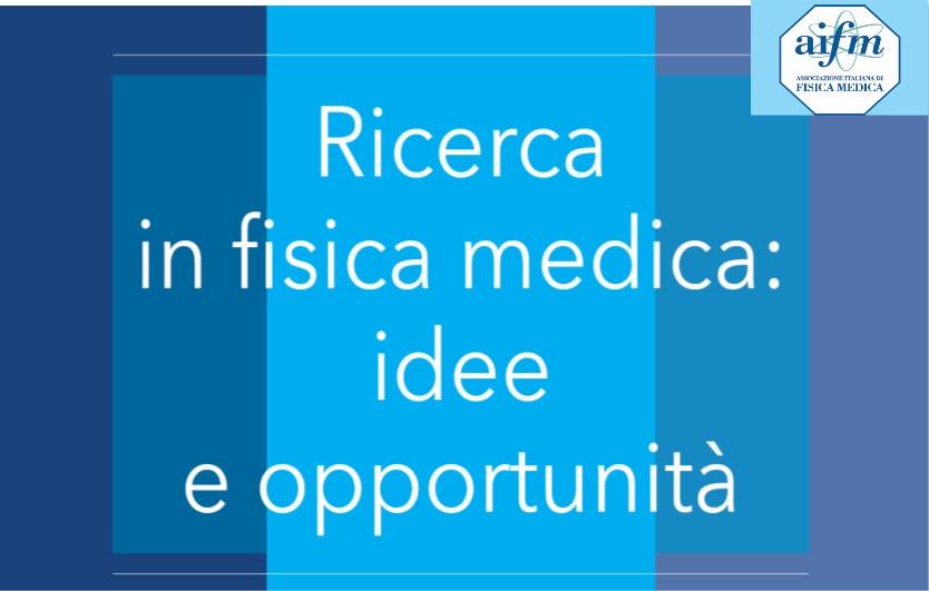
“Ricerca in fisica medica: idee e opportunità”, è il titolo del nuovo incontro interassociativ...
Usufruire delle tecnologie sviluppate dall’INFN e dal CERN ora è un’opportunità concreta per m...
La ricerca di base dà i suoi frutti accrescendo le nostre conoscenze e sviluppando tecnologi...

Il CERN e l’INFN hanno firmato oggi un accordo per lo sviluppo di una rete di Business Incubation ...
Il processo di trasferimento tecnologico facilita l’integrazione e l’applicazione pratica delle conoscenze tecnologiche, generando impatti positivi sia nell’ambito commerciale che in quello sociale.

Implementare tecnologie all’avanguardia per ottimizzare i processi produttivi, ridurre costi, migliorare la gestione e mantenere un vantaggio competitivo.

Convertire le scoperte scientifiche in soluzioni pratiche, sostenendo il processo di commercializzazione delle idee e promuovendo la collaborazione con l’industria.

Promuovere la diffusione dell’innovazione per migliorare i servizi pubblici, sostenendo lo sviluppo socio-economico e ottimizzando l’efficienza dei processi amministrativi.

Mette a disposizione materiale informativo che illustra gli impatti generati dal Trasferimento Tecnologico e fornisce informazioni utili sui i bandi attivi e le proposte in corso.
Implementare tecnologie all’avanguardia per ottimizzare i processi produttivi, ridurre costi, migliorare la gestione e mantenere un vantaggio competitivo.
Convertire le scoperte scientifiche in soluzioni pratiche, sostenendo il processo di commercializzazione delle idee e promuovendo la collaborazione con l’industria.
Promuovere la diffusione dell’innovazione per migliorare i servizi pubblici, sostenendo lo sviluppo socio-economico e ottimizzando l’efficienza dei processi amministrativi.
Mette a disposizione materiale informativo che illustra gli impatti generati dal Trasferimento Tecnologico e fornisce informazioni utili sui i bandi attivi e le proposte in corso.

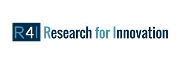
Il programma di ricerca e sviluppo dell’INFN, denominato Research for Innovation (R4I), è stato lanciato nel 2017 con l’obiettivo di ridurre la distanza tra ricerca e innovazione. Attraverso R4I, l’INFN identifica, sostiene e finanzia progetti con un notevole potenziale per elevare il proprio Technology Readiness Level (TRL), consentendo alle tecnologie di interesse per l’industria di abbreviare il tempo necessario affinché le imprese possano accedere in modo più rapido e con rischi inferiori alle tecnologie di loro interesse.
RESTA AGGIORNATO